题记,VLSI System Design 上的这篇文章其实没什么实质性的内容,只是一个特别特别笼统的概述,而且由于年久失修,某些地方的概念欠完备,但该文趣味十足,尤其是文中的手图——阐释了什么叫『简约美』,沉溺于这几张手图,所以一定要转一下,文章前半部分做了非一一对应的翻译,后半部分翻译过来比译制片都搞笑,还是看原文把,或者只看图就可以了。
题外话,关于物理设计流程,老驴曾做过大牛系列问答,每一篇都是肺腑之言经验提炼,闲时点一两篇看看,总会有收获:《玉盆纤手弄清泉 P&R问答第一篇》、《碧纱窗下水沈烟,P&R 问答第二篇》、《若似月轮终皎洁 P&R问答第三篇》、《醉里挑灯看剑 P&R问答第四篇》、《世事浮云何足问 P&R问答第五篇》、《白日放歌须纵酒 P&R问答第六篇》、《兴来今日尽君欢 P&R问答第七篇》、《锦瑟无端五十弦 P&R问答第八篇》、《去年花里逢君别 P&R问答第九篇》、《今年花开又一年 P&R问答第十篇》、《不知重会是何年:来自四旬老母的技术指导》、《QRC最佳之:顾小胖话P&R》、《金线之上的老专家 | Jason 哥》、《论P&R | 永庆告诉你》。
物理实现,可以看成是解方程,变量有:性能、功耗、面积、线长、物理规则等,『求解过程』通常被称为『 trade-off 』, 目标是在满足性能和物理规则的基础上如何尽量减小:面积、功耗、线长。
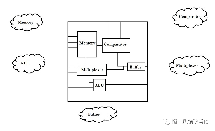
物理实现的第一步,也是最重要的一步就是floorplan, floorplan 主要做三件事儿,Floorplan 是个看功夫的活,据说在后端实现中大神跟小白最大的差距就是这一步,对于新设计不妨试一下Innovus 的mixed placement, 不论对大牛还是小白都益处多多,关于mixed placement 可以回顾《新技术 | Innovus mixed placement 几种flow》跟《新技术 | Inn Mixed Place Physical cell\, Power Routing》
- Every module has been assigned an appropriate area and aspect ratio.
- Every pin of the module has connection with other modules or periphery of the chip.
- Modules are arranged in a way such that it consumes lesser area on a chip.
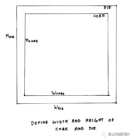
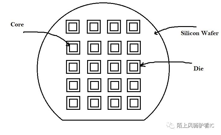
Floorplan 做完后,Chip 的面积、port 的位置、sub-block 的形状面积和pin 的位置等信息都基本确定,同时也会根据工艺和应用需求制定对应的power plan, 浅显得看chip 分为core 跟die 两部分。
"Core" 是基本逻辑单元摆放的区域,隶属于"Die"; "Die" 是IC 制造的『基本单元』,在9英寸或12英寸的wafer 上制造出成百上千颗具有某一特定逻辑功能的"Die".
注:下面一部分不翻译了,翻译过来变味,还累!
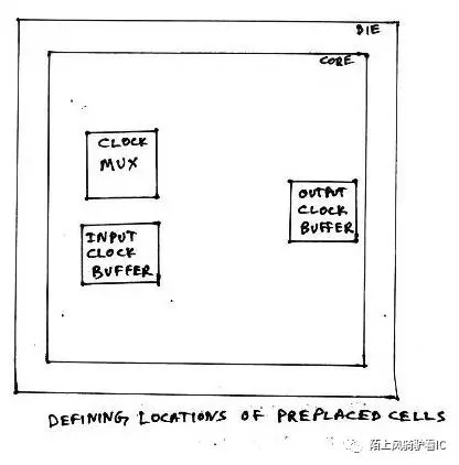
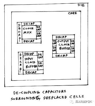
During placement and routing, most of the placement tools, place/move logic cells based on floorplan specifications. Some of the important or critical cell's locations has to be pre-defined before actual placement and routing stages. The critical cells are mostly the cells related to clocks, viz. clock buffers, clock mux, etc. and also few other cells such as RAM's, ROM,s etc. Since, these cells are placed in to core before placement and routing stage, they are called 'preplaced cells'. The above diagram describes the same.
Once the critical cells are placed on the chip, it becomes necessary to surround the critical cells by decoupling capacitors. The placement of de-coupling capacitors surrounding the pre-placed cells improves the reliability and efficiency of the chip.
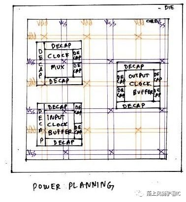
Usually, while drawing any circuit on paper, we have only one 'vdd' at the top and one 'vss' at the bottom. But on a chip, it becomes necessary to have a grid structure of power, with more than one 'vdd' and 'vss'. The concept of power grid structure would be uploaded soon. It is actually the scaling trend that drives chip designers for power grid structure.
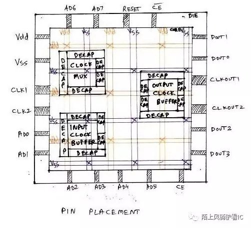
During floorplan, we define the width and height of both, core and die. The space between core and die is reserved for pin placement. For eg. an 8085 has around 40 pins viz. reset, AD0, AD1, etc. Also, the clock pins (for eg. CLK1, CLK2, CLKOUT1, CLKOUT2 in above diagram) are wider compared to other pins on the chip. It is the clock on a chip that drives most of the logic inside the chip. Hence, it should have very low resistance, and thus wide area, as resistance is inversely proportional to area.
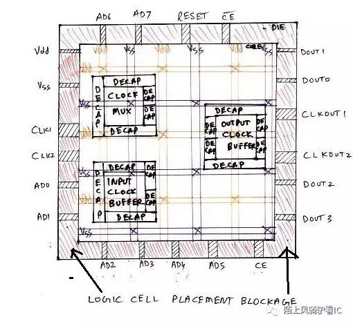
To avoid the placement of cells by placement tools, in the area between core and die (which is reserved for pin placement), it needs to be blocked by logical cell placement blockages. It is very similar to blocking a road under renovation, so that no one drives on that road, and that road is reserved for some special purpose.
Once the floorplan is freezed, it is given as an input to the placement and routing (PNR) tools. These tools are built with intelligent algorithms which would consider the design requirements (usually called as 'constraints') such as clock frequency, timing margin, max capacitance etc., calculate the location of the logical cells (Flipflops, AND, OR, BUFFER, etc) and place them in the floorplan. All the design requirements (or constraints) are stored in a single file called as 'design constraints' file, which is recognized by most of PNR tools.
Lets talk about few examples on how the built-in algorithms of PNR tools behave after detecting design constraint. The inputs to PNR tools are the design netlist, floorplan, timing libraries and design constraints. Timing libraries is a database that stores complete information about input capacitance, timing arcs, etc. of the logical cells. It also stores the list of all logical cells of different sizes.
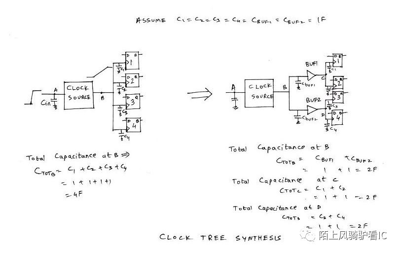
Assume, the design has a constraint which specifies that maximum capacitance on a net should not exceed 2F. Now consider the schematic in the above diagram. Clock source has a node 'B' which is connected to the 'clk' pin of 4 flip-flops. Assume that the input capacitance at 'clk' pin of each flip-flop is 1F. So now, the PNR tool built-in algorithm calculates the total capacitance on node 'B' as addition of all input capacitances at 'clk' pins of 4 flip-flops i.e 4F. Then the tool compares this capacitance number with the max capacitance constraint in the constraints file which is 2F.
Since the capacitance at node 'B' is exceeding by 2F, the tool divides the load on node 'B' through 2 buffers as shown in right side of the above figure. It selects buffers from timing library in such a way that each of those buffer has an input capacitance of 1F, and builds a tree, called as 'clock tree'. The whole process of dividing the load on clock net is called 'Clock tree synthesis (CTS)'. Above example is one of the scenarios that is considered during CTS.
The PNR tools looks for any special physical requirements from user other than timing constraints.
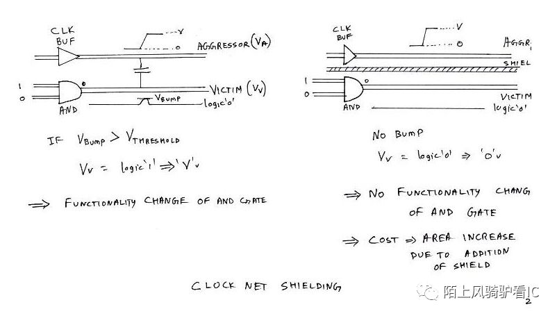
Let us create a scenario in which output net of clock buffer and output net of an AND gate are placed very close to each other, as shown in above figure. Also assume that output of AND gate is at logic '0', while the clock is switching at regular intervals. Consider clock switching from 'low' to 'high'. Since, the output net of AND gate is placed very close to the clock net, there is a high possibility that, during switching, the logic '1' might get coupled to the output of AND gate, which causes a bump with voltage 'Vbump'.
Since, a logic change or voltage level change on clock net, is causing a voltage level change on the nearby output net of AND gate, the clock net is called as 'AGGRESSOR' whereas the output net of AND gate is called as 'VICTIM'. If the bump voltage Vbump on VICTIM exceeds a certain margin or threshold, the output of AND gate switches to logic '1' which changes the functionality of the design. This phenomenon is called Crosstalk.
An efficient way to avoid the above scenario is to add a shield between VICTIM and AGGRESSOR which would break the coupling between them and hence logic level on the output net of AND gate would be retained. This requirement of adding shield around specific nets could be fed as an external input to the PNR tool. Cost paid in the above scenario would be an increase in the chip area.
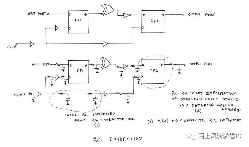
Finally when design layout is complete, the PNR tool generates a new netlist which has information about any modifications done to the original netlist, for eg. buffer addition, cell size changes, etc. It also creates a 'definition' file, which has the connectivity information between the logical cells, viz. wire length, width, locations, etc. This definition file is used to extract additional timing information due to wire inbuilt RC's (resistances and capacitances) and store them into a seperate file usually referred to as SPEF (Standard Parasitics Extraction Format) file. The design, which has the logical cells and the physical connectivity information between the cells, needs to be analysed in terms of timing i.e. the design should meet timing constraints defined by user in the beginning of PNR. Plugging the SPEF information to logical design (which is the new netlist generated by PNR tool), the complete timing information of the design is fed as an input to any Static Timing Analysis (STA) tool.
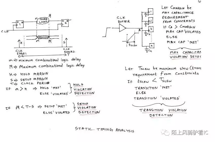
Static Timing Analysis (STA) tool helps to identify specific paths in the design which fail to meet timing requirements specified in the constraint file. These failing paths are flagged as 'VIOLATED'. There are 4 kind of checks for which the design is tested viz. Setup check, Hold check, Max Capacitance check and Transition Check. Above figure displays the scenarios under which the timing analysis tool will flag or detect violations. Once these violations are detected, it becomes necessary to analyse these violations, and plug the fixes to these violations back to the PNR netlist. This process of fixing violations by modifying the routed PNR netlist is referred to as Engineering Change Order (ECO).
作者:陌上风骑驴
原文链接:https://mp.weixin.qq.com/s/9r7U\_hrGEcKg7QEQxUfXig
微信公众号:
相关文章推荐
更多IC设计技术干货请关注IC设计技术专栏。

