

目录
原文地址:https://vlsitutorials.com/jtag-test-access-port-and-tap-controller/, 后附英文原文
Test Access Port (TAP) //测试访问接口
TAP 是 JTAG 总线的控制接口。IEEE 标准定义了四个强制的 TAP 信号以及一个可选的 TAP 信号。
- TDI (Test Data Input) –用于向目标输入数据的串行数据输入信号
- TDO (Test Data Output) – 用于从目标获取数据的串行数据输出信号
- TCK (Test Clock) – 用于 JTAG 指令/数据寄存器的测试时钟信号
- TMS (Test Mode Select) – 控制 TAP 控制器状态机状态跳变的控制信号
- [可选的] TRST (Test Reset) –用于 TAP 控制器的复位信号
TAP Controller //测试访问接口控制器
TAP controller 用于控制 JTAG 接口的行为。控制器主体是一个拥有 16 个状态的有限状态机(FSM,Finite State Machine),其状态跳变过程由 TMS 信号控制,如图 2 所示。TAP 控制器只能在 TCK 的上升沿改变状态,FSM 接下来跳转到哪个状态(next state),由 TMS 的电平以及 FSM 当前的状态(current state)决定。
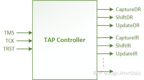
图 1- TAP 控制顶层示意图
图 1 展示了 TAP 控制器非常简略的顶层信号示意图,TMS、TCK 以及可选的 TRST 信号输入至 16 状态的状态机,根据当前状态机的状态,产生多个控制信号输出。这些输出控制信号包括指令寄存器(IR)专用的一组控制信号:
- CaptureIR
- ShiftIR
- UpdateIR
同样也为数据寄存器(DR)输出一组专用的控制信号:
- CaptureDR
- ShiftDR
- UpdateDR
以及其他一些控制信号。
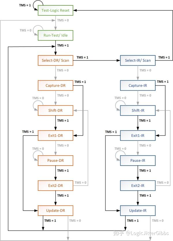
图 2- TAP 控制器 FSM 状态转移示意图
以下是关于 TAP 控制各状态的简要介绍:
• Test-Logic-Reset: 该状态时,JTAG 电路逻辑会被复位。当可选的 TRST 信号置起时,状态机返回该状态。另外,无论状态机处于何种状态,当 TMS 置为 1 并保持 5 个 TCK 时钟后,均会返回该复位状态。这样以来,即使设计中不存在 TRST 信号,也能够复位 JTAG 电路。
• Run-Test/Idle: 该状态用于表示状态机正在等待一些测试项完成。
• Select-DR/Scan and Select-IR/Scan: Select-DR/Scan 和 Select-IR/Scan 状态都是临时状态,分别用于初始化选中的 DR 或者 IR 的测试数据序列。
• Capture-DR and Capture-IR: 在这个状态中,各个寄存器并行地锁存输入端的数据。
• Shift-DR and Shift-IR: 在这个状态中,所需的数据被串行地装填到选中的寄存器中,或者从选中的寄存器中移出。如图 2 所示,TAP 控制器处于这两个状态时,当 TMS 保持为 0 时,FSM 会停留在该状态。在每个时钟周期,单个数据比特被通过 TDI 移入选中的寄存器,同时 TDO 上也会输出从目标寄存器移出的数据。
• Exit1-DR and Exit1-IR: 在这个状态中,所有并行装填的数据 (Capture-DR 和 Capture-IR 状态) ,和串行移入的数据 (Shift-DR 和 Shift IR 状态) 都在寄存器中保留。
• Pause-DR and Pause-IR: FSM 在该状态中暂时停止,以等待所需的某些外部行为完成。
• Exit2-DR and Exit2-IR: 该状态代表在 Pause-DR 和 Pause-IR 状态中暂停的行为将被恢复,TAP 控制器将返回 Shift-DR 或者 Shift-IR 状态,继续移入以及移出数据。
• Update-DR and Update-IR: 存储在第一级触发器中的数据将被锁存到第二级触发器,一般所有寄存器中的每个比特都有两级触发器组成,稍后将详细讨论这点。
原文
Test Access Port (TAP)
It is the interface used for JTAG control. The IEEE standard defines four mandatory TAP signals and one optional TRST signal.
\1. TDI (Test Data Input) – It is used to feed data serially to the target.
\2. TDO (Test Data Output) – It is used to collect data serially from target.
\3. TCK (Test Clock) – It is the clock to the registers.
\4. TMS (Test Mode Select) – It controls the TAP controller state transitions.
\5. [Optional] TRST (Test Reset) – It resets the TAP controller.
TAP Controller
It controls the JTAG operation. It is basically a 16-state Finite State Machine (FSM) whose state transitions are controlled by the TMS signal as shown in Figure 2. The TAP controller can change state only at the rising edge of TCK and the next state is determined by the logic level of TMS and the present state.
Figure 1: A top level view of TAP Controller
Figure 1 shows a very basic top-level view of TAP controller. TMS, TCK and the optional TRST signals go to a 16-state FSM, which produces various control signals depending upon the FSM’s state. These output signals include dedicated control signals for Instruction Register (IR): CaptureIR, ShiftIR, UpdateIR and generic control signals for all Data Registers (DR): CaptureDR, ShiftDR, UpdateDR along with other control signals.
Figure 2: State transition diagram of TAP Controller FSM
A brief description about the different states of the TAP controller –
• Test-Logic-Reset: It resets the JTAG circuits. Whenever the TRST (optional) signal is asserted, it goes back to this state. Also notice that in whatever state the TAP controller may be at, it will goes back to this state if TMS is set to 1 for 5 consecutive TCK cycles. Thus if we don’t have the TRST signal then we can still reset the circuit.
• Run-Test/Idle: This is a state in which the FSM is waiting for some test operations to complete.
• Select-DR/Scan and Select-IR/Scan: This is a temporary state to allow the test data sequence for the corresponding Register (the IR in Select-IR/Scan state and the selected DR in Select-DR/Scan state) to be initiated.
• Capture-DR and Capture-IR: In this state, data can be loaded in parallel to the corresponding Register
• Shift-DR and Shift-IR: In this state, the required test data is loaded (or unloaded) serially into (or from) the corresponding Register. If you refer the Figure 2, when the TAP controller is in this state, it will stay at this state as long as TMS=0. For each clock cycle, one data bit is shifted into (or out of) the selected Register through TDI (or TDO).
• Exit1-DR and Exit1-IR: All parallel-loaded (from the Capture-DR and Capture-IR state) or serial-loaded (from the Shift-DR and Shift IR state) data are held in the Register in this state.
• Pause-DR and Pause-IR: The FSM pauses its function here to wait for some external operation
• Exit2-DR and Exit2-IR: This state represents the end of the Pause-DR or Pause-IR operation, and allows the TAP controller to go back to Shift-DR or Shift-IR state for more data to be shifted in (or shifted out).
• Update-DR and Update-IR: The test data stored in the first flop of Register (typically all the Registers have two flops for each bit, we will discuss about it later) is loaded to the second flop in this state.
原文:知乎
作者:LogicJitterGibbs
相关文章推荐
- [[译文] JTAG Architecture //JTAG 架构](https://aijishu.com/a/1060000...)
- FPGA单独下载<固化文件>的解决方案
- Xilinx DDS Compiler IP 使用教程
- 还在为没有项目做发愁?这几个神级开源网站,都是FPGA/IC项目
更多FPGA干货请关注FPGA的逻辑技术专栏。欢迎添加极术小姐姐微信(id:aijishu20)加入技术交流群,请备注研究方向。

