AMD Zen2,一个巨大 规模的巨无霸。采用的是先进的7nm工艺。而一个更矮的6T的标准单元库,导致的更高的逻辑密度和实现难度。
相对于14nm,7nm导致线上电阻的增大。因此花了很多力气在net的优化上,例如,先择高层金属用于关键net的绕线(线宽减少主要是底层金属)。用via ladder降低线上的电阻以及解决EM的问题。
阅读本文,感受一下超大型芯片以及先进工艺所带来的挑战
Last year AMD introduced the Zen 2 microarchitecture, the company’s second major iteration of its Zen design. Zen 2 brought significant architectural changes at both the core level and the full SoC level. Undoubtedly, a big part of this success can be directly attributed to the company’s decision to dive headfirst into TSMC’s leading-edge 7-nanometer node. The move to TSMC 7-nanometer is a pretty big aggressive move, not only because it’s such a large technology shift, but also because of the new physical challenges it brings along with it – challenges that required the entire ecosystem – such as the foundry and CAD and EDA vendors – to collaborate on resolving those issues. At the recent ISSCC 2020 conference, AMD delved into some of those challenges in a little more detail.
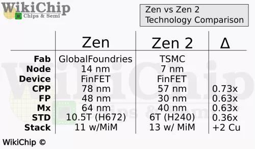
Compared to AMD’s original Zen process which was the 14-nanometer FinFET process by GlobalFoundries, TSMC 7-nanometer represents a more-than-one generational leap in terms of density which provided the designers with significantly higher transistor budget per fixed area of silicon. Additionally, AMD switched from using a high-performance cell library to using TSMC 6T library which brought a whole new set of challenges especially when it comes to routing a high-performance SoC. We have covered both processes extensively on WikiChip so for brevity’s sake a short comparison is provided below.
Perhaps the biggest difference is the switch from a fairly tall cell to a high-density short cell. Those of you who are a bit more familiar with the previously-reported Zen numbers may notice that there are a couple of discrepancies between what’s shown in the table and what AMD previously reported. The reason is that actually AMD used both 10.5T and 9T cells. The table above, and the data AMD provided, is just an assortment of key features. It’s also worth noting that AMD is using a slightly more relaxed metal stack as compared to the usual high-density metal stack so actually the overall density is a bit more relaxed than the most aggressive 6T density.
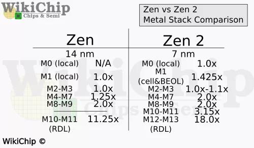
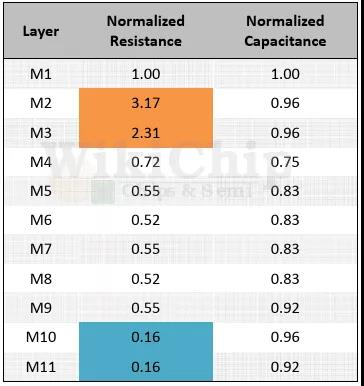
When looking at the metal stack, the 7-nanometer process offered two additional Cu layers (though later Zen also added another layer). The table below shows the pitch spacing for each of the metal lines in the stack, normalized by the respective node gate. Inside the standard cell, TSMC N7 offers a local cell interconnect layer (M0) which they did not have before. The metal 4 to 7 layers are slightly larger, and the metal 10-11 are the new metal layers that were added in that node.
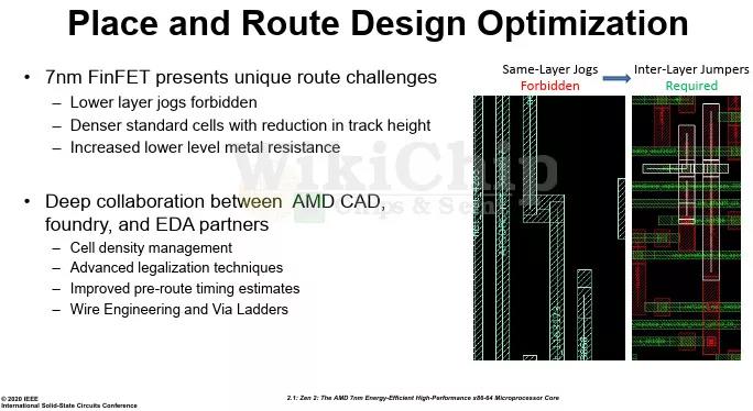
One of the challenges that needed to be addressed when they transitioned from 14 nm to 7 nm is the patterning of the lowest layers. We have talked about those differences in priors articles. In AMD’s talk, Teja Singh reiterated some of those new restrictions. Since the lower-level metals are aggressively multi-patterned, the bidirectionality that was offered by earlier nodes is now forbidden in N7. Simple layer jogs now meant you have to climb up the stack, go to where you want to go, and then go back down. This change also introduces some stray electrical properties into the cell such as extra RC.
The shorter cells gave AMD unique challenges as well. Shorter cells have the benefits of power and density, but at the same time, they come at significant complexity to place and routing. This is compounded by the unidirectionality requirements and the tight DRC rules along with the significantly higher wire resistance. Making the cells very wide, you end stressing the M1 power grid. This means that in Zen 2, large cells such as a multi-bit flip-flop ends up going taller. Upwards of eight-row tall cells is not uncommon in Zen 2. The downside of this approach is that you end up with higher fragmentation, lowering the utilization of your area (you end up with lots of dead space). Teja says that AMD had to work closely with the EDA tools providers to work through those challenges. One example was the need to do multiple passes and filling the empty areas with smaller components. Additionally, AMD implemented a number of different power grid options, allowing for more fine-grained optimizations such as an EM/IR dense grid for critical areas and a light-grid for less critical areas.
Fighting The Resistance
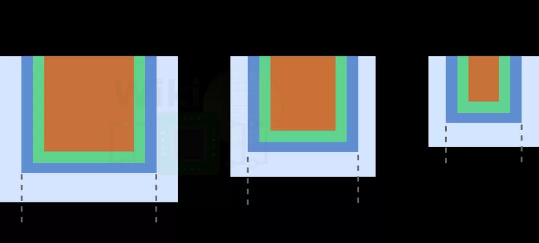
With the tighter metal pitches, 7nm brought additional challenges when it came to resistance. This isn’t new. Resistance has been a challenge for quite some time. Recent nodes have shrunk the metal pitches to a point where the barrier and liners are pretty much as thin as we can make them therefore what’s actually shrinking the copper core itself. Less copper means the barriers and liners are making up a bigger part of the wire. In other words, as the copper core continues to shrink without other aspects of the wire, the overall resistivity of the wire will continue to rise.
What’s new in 7-nanometer is that it’s accelerating – and fast. While the capacitance is still largely under control and even in 7 nm the normalized capacitance across all the metal layers is fairly uniform, the resistance is not. Far from it. Going from 16 nm to 7 nm you are looking more than 3x in your metal R. And by the way, from 7 nm to 5 nm designers are reporting a similar jump in the line resistance. AMD showed a nice graph of their Zen 2 normalized resistance and capacitance and the differences are quite large. If you look at the M2 and M3 layers, you are looking at 2.3x and 3.2x the normalized resistance. The lack of uniformity of the normalized resistance of those two layers alone is throwing a monkey wrench into assumptions that the EDA tools are making. Now you get pretty bad results due to pre-route and post-route miscorrelations.
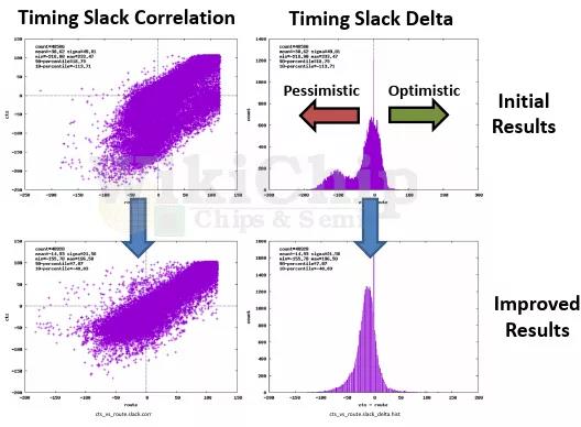
The underestimation of the M2-M3 normalized resistance is shown in the graph below which compares the route timing to the ClockTreeSynthesis. The actual values are not really important but what’s clear from the graph is that there are a lot of routing paths that were too optimistically estimated in terms of delays. Those paths have to be further optimized. Again, resolving these issues required close corporation with CAD and EDA vendors. The solution was introducing a new statistical method that took into account the placement details along with the driver location to generate better routing estimates. The results are quite good, the deviation is a lot tighter and the routing paths is leaned towards being slightly pessimistic which is where you’d want to be. It’s also worth noting that the graph shown is not the final product but rather a snapshot in time.
Wire Engineering
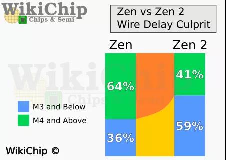
In the past, we have talked about the wire resistivity challenges that are impacting all recent leading-edge process technology designs. One thing we normally don’t have is visibility as to how profound this really is in real high-performance SoCs. The delay of the few bottom layers now contributes more to the wire delay than all the rest of the layers. In fact, the wire delay contribution at the M3 layer and below has increased from 36% on Zen to 59% on Zen 2. The changes meant there was a need to get EDA tools to understand this problem and being able to model it and optimize routing to avoid those issues. If that wasn’t enough, AMD was also targeting higher Fmax, compounding the wire problems. Manual buffering and pre-routing critical nets works, but only for a tiny subset of the chip. A more general fix was needed.
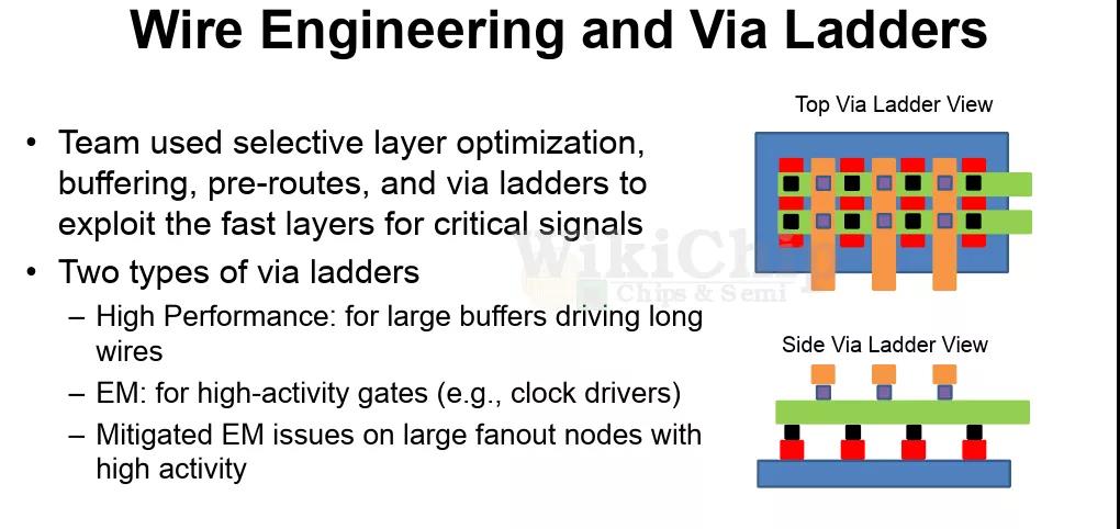
As a more generalized solution, AMD went with via ladders. We have seen TSMC talk about this a lot when it comes to their 5-nanometer node as this technique becomes even more important. TSMC calls them Via Pillars (VPs). The technique itself is not particularly new, but its ubiquitousness in new designs due to wire constraints is. Ladders are tightly-spaced identical via pairs placed in the main direction of the metal lines in a lattice structure.
The parallel mesh of wires and vias helps reduce the via resistance and the overall metal resistance at the driver, allowing to get to the higher metals faster. Similarly to the power grid, AMD had multiple implementations of the ladders – one for high performance driving long nets and one for high activity with extra electromigration mitigations.
Growing Challenges Ahead
AMD leveraging TSMC 7-nanometer process significantly boosted their capabilities in terms of what they could achieve. The catch, of course, is that the highly compelling advantages are not free. Far from it. They come with serious physical design challenges that required an ecosystem-wide collaboration from AMD, TSMC, CAD, and EDA vendors to resolve. The result is clearly worth the effort as Zen 2 delivers substantial improvement in both absolute performance and power. Looking further, AMD next-generation, Zen 3, will be leveraging TSMC 7nm+ which is an EUV-based process. That node is not a density play but instead offer a cost, learning, and refinement advantages. It’s possible that some of the challenges from N7 are actually a bit more relaxed with 7+. One such restriction is the bidirectionality constraint. Samsung did just that with their 7LPP EUV process. Unfortunately, such benefits will be very short-lived. With Zen 4 likely utilizing TSMC 5 nanometer node, the challenges from N7 will only be exacerbated.
原文链接:https://fuse.wikichip.org/news/3320/7nm-boosted-zen-2-capabilities-but-doubled-the-challenges/
作者:白山头
来源:https://mp.weixin.qq.com/s/zf...
作者微信公众号
相关文章推荐
更多IC设计技术干货请关注IC设计技术专栏。

