

原文地址:https://vlsitutorials.com/jtag-instruction-register-and-instruction-decoder/, 后附英文原文
Instruction Register (IR) //指令寄存器
指令寄存器的目的是通过 TDI 信号移入指令。另外,指令寄存器还可以在新指令完全移入之前,存储当前的指令。
一般情况下,一个 IR 会图 1 中的那样,包含两个寄存器。Hold 寄存器存储的是前一条指令,Shift 寄存器用于在不影响前一条指令的情况下,移入下一条指令。
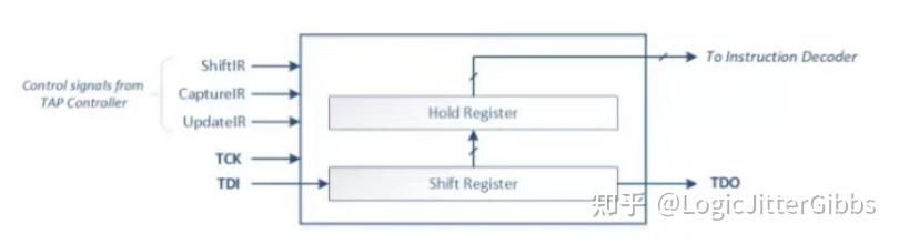
图 1- 数据寄存器顶层示意图
指令寄存器的控制信号来自于 TAP 控制器,具体的控制信号数值取决于当前 FSM 状态机的状态,使指令寄存器工作 Shift 寄存器移入/移出指令(即 Shift-IR 状态下的串行更新过程),或者使 Shift 寄存器的内容传递到 Hold 寄存器中(即 Update-IR 状态下的并行更新过程)。
假设一个 4 比特长度的指令寄存器,如果要向其中装填的一个数值,比如 4‘b1100,那么需要以下几个步骤:
- 控制 TMS 信号输入以下序列,使状态机从 “Test Logic Reset” 状态转入 "Shift-IR" 状态:
TMS = 0 (1st clock)
TMS = 1 (2nd clock)
TMS = 1 (3rd clock)
TMS = 0 (4th clock)
TMS = 0 (5th clock) - 在 "Shift-IR" 状态时,在接下来的 3 个时钟周期内保持 TMS = 0,并通过 TDI 串行移入指令数值(4'b1100)。
NOTE:这里使用 3 个时钟周期就移入了 4 比特数据,这是因为数据 4'b1100 的 LSB (即比特 0)在第四个时钟周期后出现在 TDI 端口上,这样在第五个时钟周期 FSM 进入"Shift-IR" 状态时就会将 LSB 移入。最终,数据的最后一比特 MSB 会在第八个时钟周期移入。可以参照后续章节中的示例,以更深入了解这个过程。 - 控制 TMS 信号输入以下序列,使状态机从 "Shift-IR" 状态移入 “Update-IR” 状态:
- 在 FSM 进入 “Update-IR” 状态后,Shift 寄存器中的数值(4'1100)会并行地被加载到 Hold 寄存器。此时,该指令将可以被指令译码器读取。
TMS = 1 (9th clock)
TMS = 1 (10th clock)
Instruction Decoder //指令译码器
指令寄存器(IR)中的指令会被传输给指令译码逻辑,译码逻辑会根据指令选取下一步 JTAG 操作的目标数据寄存器。我们给每个数据寄存器都分配了一个不同的指令码数值。当选择某个数据寄存器时,会将其对应的指令装填到指令寄存器中,随后指令译码器将译码该指令码,并建立其一条 TDI/TDO 和对应数据寄存器之间的通路。
假设我们的 JTAG 模块中有两个数据寄存器 DR-1 和 DR-2,以及一个 4 比特宽度的指令寄存器。所以我们将给每个数据寄存器指定一个指令码以及对应的指令,比如:
- DR-1 ( opcode = 4’b0010)
- DR-2 ( opcode = 4’b0011)
NOTE:采用 4 比特指令码,是因为该 JTAG 指令译码器位宽为 4 比特。
如果我们想通过 JTAG 访问 DR-2,那么我们需要在指令译码器中装填数值 4'b0011,指令译码器将可以译码该数值,并选中 DR-2。
原文
Instruction Register (IR)
The purpose of Instruction Register is to shift in instruction through TDI and having the provision to store the instruction till a new instruction is fully shifted in.
Typically an IR has two registers inside it as shown below. The Hold Register stores the previous instruction and the Shift Register is used to shift-in the next instruction without affecting the previous instruction’s execution.
Figure 1: A top level view of Instruction Register (IR)
The control signals to the Instruction register originates from the TAP controller and depending upon the FSM state can either cause a shift-in/shift-out through the Shift Register (serial update operation in Shift-IR state ), or cause the contents of the Shift Register to be passed across to the Hold Register (parallel update operation in Update-IR state).
Suppose we have a 4 bit instruction register and we want to load a value, say 1100 to it. Then we have to follow the steps below –
\1. Move to “Shift-IR” state from the initial “Test Logic Reset” state by applying –
- TMS = 0 (1st clock)
- TMS = 1 (2nd clock)
- TMS = 1 (3rd clock)
- TMS = 0 (4th clock)
- TMS = 0 (5th clock)
\2. While in “Shift-IR” state, keep TMS = 0 for the next 3 clock cycles to serially shift-in the data (1100) through TDI.
NOTE: 3 clock cycles to shift 4 bits data because the LSB (logic 0) of data 1100 was made available in the TDI port after 4th clock, thus in the 5th clock itself the LSB was loaded when the FSM entered the “Shift-IR” state. The MSB (logic 1) of data 1100 was shifted in 8th clock. You can refer the example shown here for a better understanding.
\3. Move to “Update-IR” state from the “Shift-IR” state by applying –
- TMS = 1 (9th clock)
- TMS = 1 (10th clock)
When the FSM entered the “Update-IR” state, the data (1100) in the Shift Register was loaded to the Hold Register in parallel. Thus the instruction is now made available for the instruction decoder.
Instruction Decoder
The instruction from the Instruction Register (IR) is fed to a decoder logic, which selects the Data Register for JTAG operation. We assign a unique value (or opcode) to each and every Data Register in the JTAG. In order to select a Data Register, we load the IR with the corresponding opcode and the Instruction Decoder decodes the value and establishes an access path between the TDI/TDO and the required Data Register.
Suppose we have two Data Registers DR-1 and DR-2, and a 4 bits Instruction Register in our JTAG. So we will assign opcodes to the Data Registers and specify the same to the IR
DR-1 (say opcode = 4’b0010) DR-2 (say opcode = 4’b0011)
NOTE: 4 bits opcode, because the IR is 4 bits.
If we want to access DR-2 for any JTAG operation, then we have to load the instruction register with a value 4’b0011 and the instruction decoder will be able to decode this value to select the DR-2.
原文:知乎
作者:LogicJitterGibbs
相关文章推荐
- [[译文] TAP and TAP Controller // JTAG 测试访问接口及其控制器](https://aijishu.com/a/1060000...)
- [[译文] JTAG Architecture //JTAG 架构](https://aijishu.com/a/1060000...)
- FPGA单独下载<固化文件>的解决方案
- Xilinx DDS Compiler IP 使用教程
更多FPGA干货请关注FPGA的逻辑技术专栏。欢迎添加极术小姐姐微信(id:aijishu20)加入技术交流群,请备注研究方向。

