
目录
原文地址:https://vlsitutorials.com/dft-scan-and-atpg/, 后附英文原文
芯片制造厂家的工艺一般多多少少会导致芯片存在一些缺陷(defects),这些缺陷通常被称为故障(fault)。如果有详细定义的测试流程能够让这些故障在实际硅片上暴露出来,那么这些故障被认为是可测试的(testable)。为了能够在测试中尽可能检测到多的故障,我们需要在测试中增加额外的逻辑。DFT (Design for testablility)就指这些能够使完成检测任务尽可能可行的设计技巧。本文中将讨论最常见的逻辑测试 DFT 技术,它们包括 Scan 和 ATPG。在讲述这两项技术的基础知识之前,让我们首先理解故障模型(fault model)的概念。
Fault Models //故障模型
故障模型是制造缺陷导致的故障现象的抽象描述,用于生成测试向量去检测这些缺陷。缺陷及故障模型包括:
- Functional Defects : Stuck-at Fault Model //功能性缺陷: Stuck-at 故障模型
- Current defects : Pseudo Stuck-at Fault Model (IDDQ) //电流缺陷:Pseudo Stuck-at 故障模型(IDDQ)
- Speed defects: At-speed Fault Model, Path Delay Fault Model //速度缺陷:At-speed 故障模型,路径延迟故障模型
但是,本文只会讨论前两项最为常见的故障模型:stuck-at 以及 at-speed 故障模型。
Stuck-at Faults // Stuck-at 故障
这是生产中最常见的故障模块。它建模描述了生产中将电路某个节点永久性地和 VDD 短路(stuck-at 1 故障)或者和 GND 短路(stuck-at 0 故障)等情况。故障可能发生在逻辑门的任意输入或者输出端,因此一个 2 输入的与门会遇到 6 种可能的 stuck-at 故障。
在如图 1 所述的电路中,假设我们在与门输出端有一个 stuck-at-0 故障。值得注意的一点是,因为电路有三个输入端口,因此电路有共计 8 种输入组合,它们是 {000, 001, 010, 011, 100, 101, 110, 111};在这 8 种组合之中,只有两种组合可以测试出这个故障: {011, 111} ,因为其他组合的输出结果和存在 s-a-o (stuck-at 0 )故障时的输出结果相同。我们可以轻松地推断出可用的故障检测输入组合,因为这是一个非常简单的电路,但是如何找出更大电路的故障检测输入组合呢?我们不需要太担心这点,CAD 工具(ATPG 工具)会帮我们完成这项工作。ATPG 工具会通过复杂的算法,尝试生成能检测出所有 stuck-at 故障的输入组合,如果生成的输入组合无法检测出某些故障,那么这些故障会被分类至 untestable 故障。
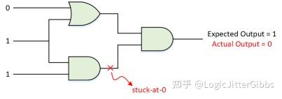
图 1:存在 stuck-at-o 故障的电路
At-speed Faults // At-speed 故障
At-speed 故障模型建模描述了芯片生产过程造成的门电路输入端口到输出端口存在严重延迟的缺陷。针对这种故障,每个输入端口都会分别测试逻辑 0 到 1 跳变(slow-to-rise 故障),和逻辑 1 到 0 跳变(slow-to-fall 故障)。和 stuck-at 故障一样,这些 at-speed 故障可能存在于门的任意输入端口或者输出端口,因此一个简单的 2 输入与门存在 6 种可能的 at-speed 故障情况。
在如图 2 所述的电路中,假设我们在与门输出端有一个 slow-to-fall 故障。从电路图中可以看到,与门输出端的更慢的 1 到 0 跳变会影响 Flop2 在其捕获时钟边沿捕获的数值。我们可以通过将 Flop 1 的初值设为 1,搭配 010 的输入组合检测到这个错误。和 stuck-at 故障检测输入组合相同,ATPG 工具也能够根据需求,生成覆盖所有可能的 at-speed 故障发生点的测试向量。
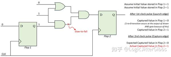
图 2:存在 slow-to-fall 故障的电路
Scan and ATPG
Scan 是一种通过改变内部电路连接方式,以增加可测试性技术的方法。ATPG 是 Automatic Test Pattern Generation 的缩写,正如其名字表达的那样,ATPG 是自动生成 Pattern 的工具。从另一个角度来说,Scan 电路能够使检测上述故障的测试向量生成过程更加容易。
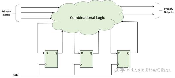
图 3:一个典型的时序电路(在 scan insertion 之前)
上述的 stuck-at 和 at-speed 故障的测试需要在测试之前,将触发器输出值初始化为需要的数值。在更大规模的时序电路(未插入 scan 的情况)中,通过顶层输入端口控制所有触发器的输出值,并通过顶层输出端口观测捕获结果是很困难的。为了解决这个问题,我们在综合期间会进行 Scan 插入(Scan Insertion)的操作。
Scan 插入的目的是将难以测试的时序电路行为,转变为类似易于测试的组合逻辑电路的行为。实现该目标需要完成以下两个步骤:
1. Converting Regular Flop to Scan Flop // 将普通的 FF 转变为 Scan FF
所有设计中使用的触发器都将替换为 Scan 触发器(结构如图 4 所示),除了下述两种触发器:
- 由用户从 scan 列表中排除的触发器,它们又被称为 non-scan 触发器。
- 存在 DFT 设计规则检查(DRC)错误的触发器。
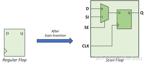
图 4: 普通触发器 vs Scan 触发器
2. Stitching the Scan Flops to form Scan Chains // 连接 Scan 触发器组成 Scan Chain
Scan 触发器被连接起来,形成了一个扫描链(如图 5 所示),设计中的扫描链数量取决于以下这些用户输入设置:
• Length of scan chain // 扫描链长度 • Clock domain mixing //时钟域混合情况 • Power domain mixing //电源域混合情况 • Voltage domain mixing //电压域混合情况
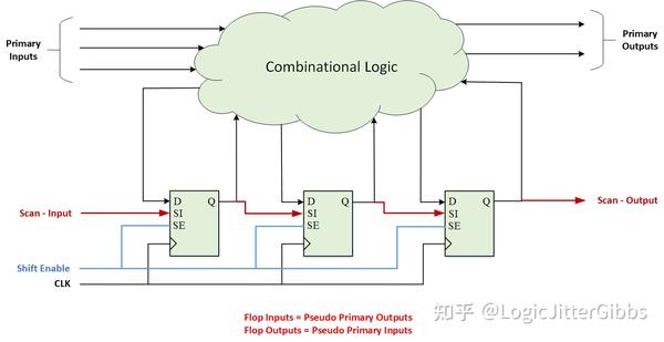
图 5:一个典型的适用于 Scan 和 ATPG 的时序电路(在 scan insertion 之后)
为了设置触发器初值(如图 5 所示),我们使 SE = 1,激活 SI 到 Q 端的路径,这样就可以通过设计顶层的主输入端口(primary input)把想要的数值串行地移入,这些端口被称为 Scan Input。在将数值移入到触发器后,我们通过设置 SE = 0,获取组合逻辑在当前输入下的输出值。然后,再次设置 SE = 1,串行地通过设计顶层的输出结果移出,以观测输出值。这些输出端口被称为 Scan Output。这时,我们将触发器的输出 Q 端称为设计的伪主要输出端口,将触发器的输入 D 端称为设计的伪主要输入端口,也就是说此时这些时序逻辑成为了一个“伪” 组合逻辑。
在硅前(pre-silicon)阶段,当测试向量生成完毕后,我们同时可以生成预期的测试结果。在硅后阶段,预期测试结果和测试向量一起存储在 ATE 的内存中。测试芯片时,测试机台将加载测试向量,并将测试结果和预期比较,判断测试向量是否通过。
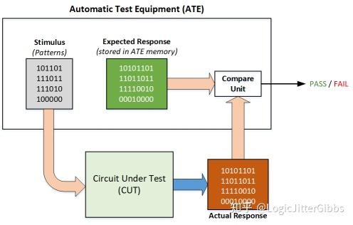
图 6:如何测试的示意图
原文
The chip manufacturing process is prone to defects and the defects are commonly referred as faults. A fault is testable if there exists a well-specified procedure to expose it in the actual silicon. To make the task of detecting as many faults as possible in a design, we need to add additional logic; Design for testability (DFT) refers to those design techniques that make the task of testing feasible. In this article we will be discussing about the most common DFT technique for logic test, called Scan and ATPG. Before going into Scan and ATPG basics, let us first understand the concept of fault model.
Fault Models
Fault models abstract the behavior of manufacturing defects so that test vectors can be generated to detect them.
• Functional Defects : Stuck-at Fault Model • Current defects : Pseudo Stuck-at Fault Model (IDDQ) • Speed defects: At-speed Fault Model, Path Delay Fault Model
However in this article we will be discussing about two most common fault models: stuck-at and at-speed fault models.
1. Stuck-at Faults
This is the most common fault model used in industry. It models manufacturing defects which occurs when a circuit node is shorted to VDD (stuck-at-1 fault) or GND (stuck-at-0 fault) permanently. The fault can be at the input or output of a gate. Thus a simple 2-input AND gate has six possible stuck-at faults.
In the circuit shown in Figure 1, suppose we have a stuck-at-0 fault at the output of an AND gate. Note one important thing, there are three input ports in the circuit, thus we can have a combination of eight different inputs or patterns {000, 001, 010, 011, 100, 101, 110, 111}; out of the eight patterns, only two patterns {011, 111} will be able to detect this fault because with rest of the patterns the expected output will be same as the actual circuit output in the presence of this s-a-0 fault. This is a small circuit so we can easily find the pattern that can detect this fault, but what about much bigger circuits? Well we don’t have to worry about it as the CAD tools (ATPG tools) will do that for us. The ATPG tools will try to generate the stuck-at fault patterns required to test all the possible fault locations using complex algorithms, but if it is unable to find patterns for few faults, then it will classify those faults as untestable.
Figure 1: stuck-at-0 fault in a circuit
2. At-speed Faults
It models the manufacturing defects that behave as gross delays on gate input-output ports. So each port is tested for logic 0-to-1 transition delay (slow-to-rise fault) or logic 1-to-0 transition delay (slow-to-fall fault). Like stuck-at faults, the at-speed fault can be at the input or output of a gate, thus a simple 2-input AND gate has six possible at-speed faults.
In the circuit shown in Figure 2, suppose we have a slow-to-fall fault at the output of an AND gate. As shown, a slower 1-to-0 transition at the output of AND gate can affect the value captured by the Flop 2 at its capture edge. It is important to note that only with an initial state ‘1’ in Flop 1 and 010 at the input, we will be able to detect this fault. And like stuck-at fault pattern generation, the ATPG tools will try to generate the at-speed fault patterns required to test all the possible fault locations.
Figure 2: slow-to-fall fault in a circuit
Scan and ATPG
Scan is the internal modification of the design’s circuitry to increase its test-ability. ATPG stands for Automatic Test Pattern Generation; as the name suggests, this is basically the generation of test patterns. In other words, we can say that Scan makes the process of pattern generation easier for detection of the faults we discussed earlier.
Figure 3: A typical sequential circuit (before scan insertion)
To test a fault we need to initialize the flops to the required values as we had shown while discussing about stuck-at faults and at-speed faults. In a bigger sequential circuit (without scan), it is difficult to control the flop’s value through primary inputs and observe the captured response in primary outputs. To solve this issue we do ‘Scan Insertion’ during synthesis.
The goal of ‘Scan Insertion’ is to make a difficult-to-test sequential circuit behave (during testing process) like an easier-to-test combinational circuit. Achieving this goal involves two steps –
1. Converting Regular Flop to Scan Flop
All the flops in the design are converted into scan flops (as shown in Figure 4), except – • The ones that are excluded by user. These are called non-scan flops. • The ones that have DFT DRC violation(s).
Figure 4: Regular flop vs Scan flop
2. Stitching the Scan Flops to form Scan Chains
The scan flops are stitched to form scan chain(s) (as shown in Figure 5). The number of scan chains depends upon various user inputs like – • Length of scan chain • Clock domain mixing • Power domain mixing • Voltage domain mixing
Figure 5: A typical sequential circuit compatible for Scan and ATPG (after scan insertion)
To initialize any flop to a value (refer the Figure 5), we simply make the SE = 1, such that SI to Q path is activated and we shift in the required values serially through a top level primary input called Scan-Input. Once the required values are loaded to the flops, we capture the values from combinational circuit by making SE = 0. And to observe the captured response we make the SE = 1 and serially shift out the captured data through a primary output called Scan-Output. Thus in a way, we can say the scan flop’s output (Q) act as pseudo primary output of the design and the scan flop’s input (D) act as pseudo primary inputs to the design, thereby making it a pseudo combination circuit.
Once the patterns are generated, the expected response of the circuit for each pattern is obtained in pre-silicon. The expected responses along with the patterns are then stored in the memory of Automatic Test Equipment (ATE). In post-silicon, the manufactured chip is tested using the ATE, which loads the pattern and compares it with the expected response for pass or fail status.
Figure 6: A schematic showing how testing works
原文:知乎
作者:LogicJitterGibbs
相关文章推荐
- 【译文】 Example showing JTAG Operation // JTAG 运行示例
- JTAG Architecture //JTAG 架构
- FPGA单独下载<固化文件>的解决方案
- Xilinx DDS Compiler IP 使用教程
- 还在为没有项目做发愁?这几个神级开源网站,都是FPGA/IC项目
更多FPGA干货请关注FPGA的逻辑技术专栏。欢迎添加极术小姐姐微信(id:aijishu20)加入技术交流群,请备注研究方向。

