目录
原文地址:https://vlsitutorials.com/dft-scan-clocking-architecture/, 后附英文原文。
如果电路设计中只考虑电路的功能性,而没有考虑可测试性,那么需要更改时钟架构,才能支持 Scan 相关测试的运行。本文将以修改一个非常简单的纯功能性(functional)电路的时钟架构,以适应 Scan 需求的例子,来说明时钟结构为增加可测试性所需的修改。
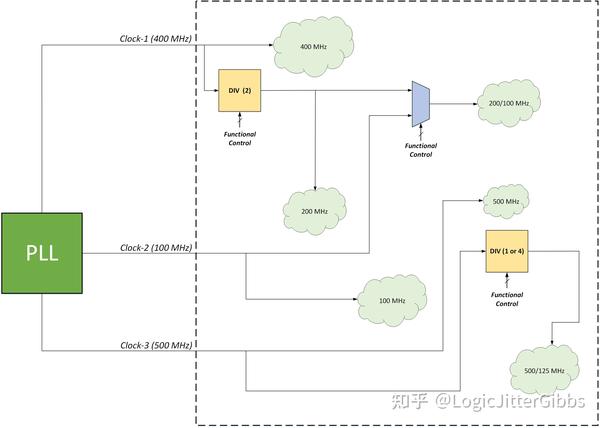
图 1: 一个未考虑 scan 测试需求的功能性时钟架构示例
The given scenario //初始时钟架构
如图 1 所示,有一个能够产生三种不同频率时钟的 PLL(三个时钟频率分别为 500 MHz, 400 MHz 和 100 MHz)。图中不同的云朵状图形表示不同的时钟域(其中包括待测试的逻辑)。
图中还有两个分频器(divider):
- DIV(2),该分频器始终将输入时钟二分频,所以其输出的时钟频率为 200Mhz。
- DIV(1 or 4),该分频器可以选择将输入时钟四分配,或者不分频直接将输入时钟旁路输出,选择取决于功能上的需求。所以,该分频器输出端的时钟可能是 500MHz 或者 125MHz。
一般情况下,分配器由功能性电路选择分频系数。本例中的 DIV(2)分频器相当于分频系数固定为 2。在多数具体实现中,除了复位信号以外,这类分频器的控制信号都会使用固定的高电平或者低电平。但对于分频系数可能为 1 或者 4 的 DIV(1 or 4)分频器,其分频系数选择一般在功能模式下由一个状态机(或者其他控制逻辑)控制。
图中还有一个时钟选择器(mux),在功能模式下由控制电路选择两路输入时钟中的一路时钟从输出端向后级传播。mux 输出端可能输出 200MHz 频率的时钟(来自分频器输出),或者 100MHz 频率的时钟(来自 PLL 输出)。和分频器的控制逻辑一样,mux 在功能模式下由一个状态机(或者其他控制逻辑)控制。
Modifications required //测试模式所需的时钟架构修改
接下来让我们一一道来原设计在时钟架构上所需要的修改,使设计对 Scan 更加友好。
在 stuck-at 测试中,时钟域的频率对测试是无关紧要的(译注:会统一使用相对低速的 scan clock)。但是在 at-speed 测试中,我们需要在每个时钟域的最高频率下进行测试,原因在at-speed 相关文章中所述。图 4 时钟域的云朵形状中用红色文字标记出了这个时钟域的最高频率。
测试模式控制信号
设计中包含 2 个分频器和 1 个时钟选择器,我们需要在 at-speed 测试期间保证他们输出正确频率的时钟,即最高频率的时钟。
clock mux
mux 输出端可能输出的最高频率时钟是 200MHz,因为控制 mux select 信号的 FSM 也是 scan chain 的一部分,所以 FSM 输出的 mux select 信号在测试期间可能会不断跳变(toggle)。因此,mux 输出端的时钟就变得不确定,某个时刻输出时钟可能是两个输入端时钟中的任意一个。 为了防止这种影响测试的现象发生,我们需要如图 4 所示,在 mux 的 select 端再加一个简单的 mux。这样一来,测试模式 (Test Mode = 1) 时会屏蔽掉功能模式下的 select 信号,选择频率最高的时钟输出(此例中是 mux 的 200MHz 输入时钟)。
DIV(2)分频器
上述 mux 的 200MHz 时钟来自 DIV(2)的输出,所以在 scan 模式中 DIV(2)是测试时钟的驱动者,以使后级测试逻辑获得所需的 200MHz 时钟。但是,如果分频器本身也需要进行 scan 测试,那么分频器的内部逻辑也会被加入到 scan chain 中,那么这些信号在测试期间可能会不断跳变,导致分频器输出频率不可预知的时钟信号,所以我们不能对分频器本身进行 scan 测试。同时,分频器的 reset 或者其他功能模式下的控制信号都需要被屏蔽,因为它们可能会影响分频器在测试模式下的工作,如图 2 所示。
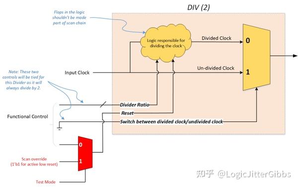
图 2:分频器 DIV(2)所需的改动示意图
DIV(1 or 4)分频器
在测试中,我们需要分频器 DIV(1 or 4)输出频率更高的 500MHz 时钟,因为我们需要屏蔽功能模式下的分频系数的控制信号,在测试模式下将其固定选择为分频的时钟输出,如图 3 所示。因为分频器在测试模式下出于旁路输出状态,因此我们可以对分频器本身进行 scan 测试,因为此时不会影响分频器的输出。
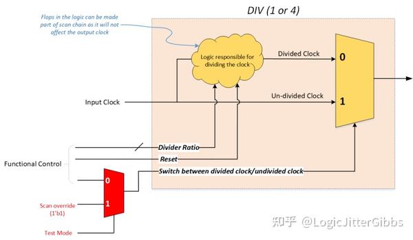
图 3:分频器 DIV(1 or 4)所需的改动示意图
增加 OCC
接下来我们需要在时钟架构中,为每个时钟域增加一个 OCC(片上时钟控制器,On-chip Clock Controller),如图 4 所示。图中存在 6 个时钟域,相应地需要 6 个 OCC。如相关文章中讨论的那样,OCC 在测试模式下根据需求控制时钟行为。
事实上,图 4 中的 scan 时钟架构示例还有进一步优化的空间,但我们要止步停下了,使其成为一个更清楚,和更本质的示例,展示了如何定义一个 scan 友好的时钟架构。
Note:需要确保分频器或者选择器的输入时钟是未受门控的(free-running),即未经过 OCC。
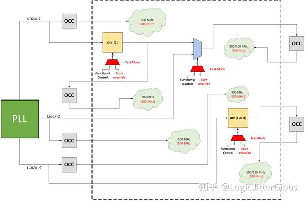
图 4:在图 1 基础上,为了支持 Scan 运行需要做的改动示意图
原文
The clocking architecture of a design needs to be modified to support ‘Scan’ operation. In this article we will take an example of a very generic functional clocking architecture as shown in Figure 1 and modify it.

Figure 1: An example of a typical clocking architecture (without considering scan testing requirement)
The given scenario –
As shown in Figure 1, there is a PLL which is generating three different clocks (of frequency 500 MHz, 400 MHz and 100 MHz). The cloud like structures in the figure indicates different clock domains (having the logic we want to test).
There are two dividers – 1. DIV (2) – which divides the input clock by 2. So the frequency of the clock at the output of divider is 200 MHz. \2. DIV (1 or 4) – which either divides the input clock by 4 or bypasses it without any division, depending upon the functional requirement. So the frequency of clock at the output of divider is either 500 MHz or 125 MHz.
The dividers have functional control that determines the division ratio of the divider. The divider ‘DIV (2)’ always divides the input clock by a constant value of 2; typically in such dividers the functional control, excluding the reset to divider is likely to be tied to a constant value in the design. But the divider ‘DIV (1 or 4)’ can either divide the input by 4 or bypass it; typically the functional control of such dividers are controlled by a FSM (or any other controlling logic).
There is also a clock mux, which has a functional control that selects which clock it should propagate at its output. The frequency of the clock at the clock mux output can be either 200 MHz (from the divider) or 100 MHz (from the PLL). Like the dividers, the functional control in a clock mux is typically controlled by a FSM (or any other controlling logic).
Modifications required –
Now let us go through the modifications needed in clocking architecture for making the design ‘Scan’ friendly –
In stuck-at testing the frequency of the clock domain we will be testing doesn’t matter; but in at-speed testing, we should be testing the clock domain at the maximum frequency it supports because of the reason discussed here. The frequency shown in red inside the clock domains (cloud like structures) in Figure 4, indicates the maximum clock frequency of that clock domain.
\1. Since we have two clock dividers and one clock mux in our design, we have to ensure the clock with the highest frequency is propagated at the output of dividers and clock mux for at-speed testing at correct frequency.
1.1. Clock mux – Maximum possible frequency at the output is 200 MHz. Since the FSM controlling the select pin of clock mux will be part of scan chains, it will toggle during testing. Hence the clock at the output of the clock mux becomes unpredictable and can be any one of its input at any instance. To prevent this, we need to add a simple mux as shown in Figure 4, which will mask the functional control in scan mode (Test Mode = 1), to select the clock with highest frequency (in this case the 200 MHz clock).
1.2. ‘DIV (2)’ – The 200 MHz clock at the output of clock mux is coming from the clock divider ‘_DIV (2)’_, thus ‘_DIV (2)’_ should function as a divider throughout the scan mode, so that we will get the required 200 MHz clock. If we scan the divider, the logic responsible for dividing the clock will become part of scan chain and will toggle during scan mode, resulting in clock of unpredictable frequency at the output of divider; so we should not scan this divider. Also we have to mask the reset or any other functional control that it likely to affect the functionality of the divider as shown in Figure 2.

Figure 2: Diagram showing the the modifications required for divider DIV(2)
1.3. ‘DIV (1 or 4)’ – We need the undivided clock of 500 MHz (fastest clock), thus we need to mask the functional control to select the undivided clock in scan mode, as shown in Figure 3. Since we are bypassing the divider, we can scan this divider as it will not affect the divider output.

Figure 3: Diagram showing the modifications required for divider DIV(1 or 4)
\2. Then we need to modify the clocking architecture to add an On-chip Clock Controller(OCC) for every clock domain, as shown in Figure 4. We have six clock domains, thus six OCCs. As discussed here, the OCC controls the clock operation required for testing a circuit.
Although the scan clocking architecture (shown in Figure 4) can be further optimized for this particular example, but this is a much cleaner and generic representation to illustrate how we need to define a Scan friendly clocking architecture.
Note: Ensure all the clock(s) to the input of a divider or a clock mux should be free running, meaning it should not be coming from an OCC.

Figure 4: Modification required in the clocking architecture shown in Figure 1, to support ‘Scan’ operation
原文:知乎
作者:LogicJitterGibbs
相关文章推荐
- 【译文】PCI Express Technology 3.0 Chapter 8 事务排序
- 【译文】 DFT, Scan and ATPG
- 【译文】 Example showing JTAG Operation // JTAG 运行示例
- JTAG Architecture //JTAG 架构
- FPGA单独下载<固化文件>的解决方案
更多FPGA干货请关注FPGA的逻辑技术专栏。欢迎添加极术小姐姐微信(id:aijishu20)加入技术交流群,请备注研究方向。


